Email:export@yangxing.hk
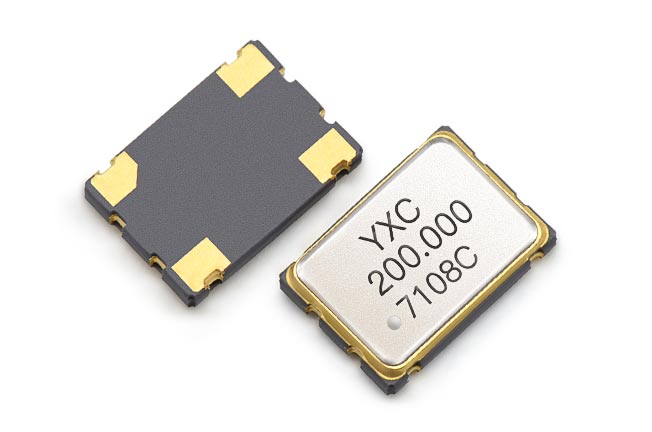
YSO690PR
Programmable Quartz Crystal Oscillator
Frequency Range:1MHz to 200MHz
Any frequency between 1MHz to 200MHz accurate to 6 decimal places
Dimensions: 2016,2520,3225,5032,7050
Rohs Status: Compliant
High stability、Low Jitter
Frequency Range:1MHz to 200MHz
Any frequency between 1MHz to 200MHz accurate to 6 decimal places
Dimensions: 2016,2520,3225,5032,7050
Rohs Status: Compliant
High stability、Low Jitter
 Download PDF
| Parameter | 1.8V | 2.5V | 3.3V |
| Frequency Range | 1MHz to 125MHz | 1MHz to 200MHz | 1MHz to 200MHz |
| Supply Voltage Variation (Vdd)10% | 1.62 V to 1.98 V | 2.25 V to 2.75 V | 2.97 V to 3.63 V |
| Standby Current | 400μA | ||
| Frequency Tolerance | ± 20 ppm, ± 25 ppm, ± 50 ppm, or specify | ||
| Output Load | 15pF, or specify | ||
| Operating Temperature Range | - 40 ~ + 85 ℃, or specify | ||
| Storage Temperature Range | -55 ~ +150 ℃ | ||
| Voltage Vol ( Max. ) / Vol ( Min. ) | VOH=90%Vdd / VOL / =10%Vdd | ||
| Duty Cycle | 45~ 55% | ||
| Period Jitter (@12K-20MHz) | 1.8V=1.5ps 2.5V=1.1ps 3.3V=1ps | ||
| Start-up Time | 7msMax. | ||
| Supply Current | See Below | ||
| Frequency Aging ( at 25 ℃ ) | ± 3 ppm / year Max | ||
Part Number Guide O97050200MEDA4SI - *
| Oscillator | Series | Dimensions (mm) |
Frequency (Hz) |
Voltage (V) |
Stability (ppm) |
Output | Pin | Material | Operating Temp | - | Remark |
| O | 9 | 7.5 x 5.0 | 200M | E | D | A | 4 | S | I | - | * |
Pin Description
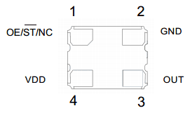
| Pin | Symbol | Functionality | |
| 1 |
OE/ST/NC | Output Enable | H : specified frequency output L : output is high impedance. Only output driver is disabled. |
| Standby | H : specified frequency output L: output is low (weak pull down). Device goes to sleep mode. Supply current reduces to I_std. |
||
| No Connect | Any voltage between 0 and Vdd or Open : Specified frequency output. Pin 1 has no function. | ||
| 2 | GND | Power | Electrical ground |
| 3 | OUT | Output | Oscillator output |
| 4 | VDD | Power | Power supply voltage |
External dimensions
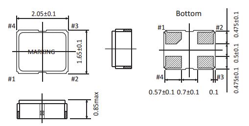 2.5x2.0x0.85mm
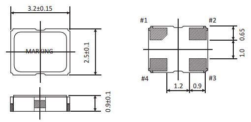 3.2x2.5x0.9mm
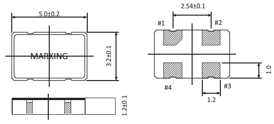 5.0x3.2x1.20mm
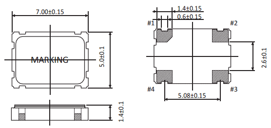 7.0x5.0x1.40mm
(Unit: mm)
SHENZHEN YANGXING TECHNOLOGY CO., LTD.
ADD:Rm 1901, 19th Floor, 1st Huide Building, Mintang Rd No.385, Longhua District, Shenzhen China
Email:export@yangxing.hk
Skype ID: 125784862


