Email:export@yangxing.hk
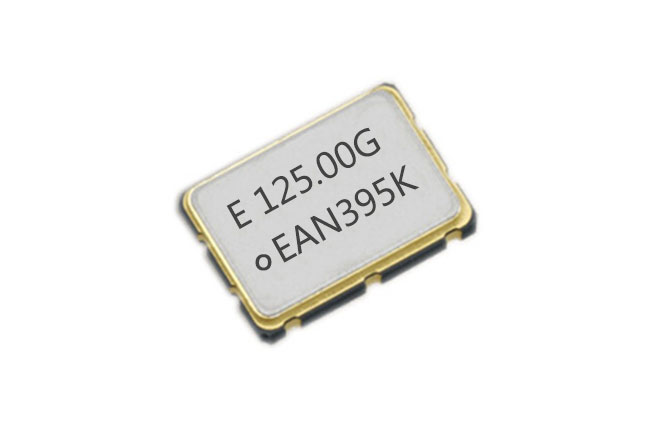
SG7050VAN
Type: Differential Crystal Oscillator
Frequency Range: 73.5MHz to 700MHz
External dimensions: 7.0*5.0mm
Rohs Status: Compliant
PN: X1G004281002400 X1G004281003300
Applications: wireless communication, PC, and LCDM
Frequency Range: 73.5MHz to 700MHz
External dimensions: 7.0*5.0mm
Rohs Status: Compliant
PN: X1G004281002400 X1G004281003300
Applications: wireless communication, PC, and LCDM
 Download PDF
| Item | Symbol | Specifications | Condition/Remarks | ||
|---|---|---|---|---|---|
| LV-PECL | LVDS | ||||
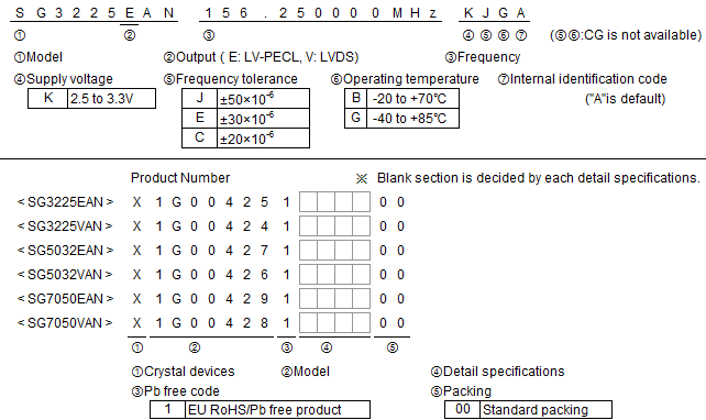
| SG3225EAN SG5032EAN SG7050EAN |
SG3225VAN SG5032VAN SG7050VAN |
||||
| Output frequency range | f0 | 73.5 MHz to 700 MHz | Please contact us about available frequencies. | ||
| Supply voltage | VCC | K : 2.5 V to 3.3 V | VCC = ±10 % | ||
| Storage temperature | T_stg | -40 °C to +125 °C | Store as bare product. | ||
| Operating temperature | T_use | B : -20 °C to +70 °C G : -40 °C to +85 °C |
|||
| Frequency tolerance | f_tol | C : ±20 × 10-6 E : ±30 × 10-6 J : ±50 × 10-6 |
|||
| Current consumption | ICC | 65 mA Max. | 30 mA Max. | OE = VCC L_ECL = 50 Ω or L_LVDS = 100 Ω f0 = 700 MHz |
|
| Disable current | I_dis | 20 mA Max. | OE = GND | ||
| Symmetry | SYM | 45 % to 55 % | At outputs crossing point | ||
| Output voltage (LV-PECL) |
VOH | VCC - 1.0 V to VCC - 0.8 V | - | DC characteristics | |
| VOL | VCC - 1.78 V to VCC -1.62 V | - | |||
| Output voltage (LVDS) |
VOD | - | 250 mV to 450 mV | VOD1 , VOD2 | DC characteristics |
| dVOD | - | 50 mV Max. | dVOD = | VOD1 - VOD2 | | ||
| VOS | - | 1.15 V to 1.35 V | VOS1 , VOS2 | ||
| dVOS | - | 150 mV Max. | dVOS = | VOS1 - VOS2 | | ||
| Output load condition (ECL)/(LVDS) |
L_ECL | 50 Ω | - | Terminated to VCC - 2.0 V | |
| L_LVDS | - | 100 Ω | Connected between OUT to OUT | ||
| Input voltage | VIH | 70 % VCC Min. | OE terminal | ||
| VIL | 30 % VCC Max. | ||||
| Rise time / Fall time | tr/tf | 350 ps Max. | - | Between 20 % and 80 % of ( VOH - VOL) | |
| - | 300 ps Max. | Between 20 % and 80 % of Differential Output peak to peak voltage. | |||
| Start-up time | t_str | 3 ms Max. | Time at minimum supply voltage to be 0 s | ||
| Phase Jitter | tPJ | 0.6 ps Max. *1 | Offset frequency : 12 kHz to 20 MHz | ||
| Frequency aging | f_aging | ±5 × 10⁻⁶ / year Max. | +25 °C , VCC = 2.5 V or 3.3 V First year. |
||
*1. f0 = 243 MHz to 250 MHz , 486 MHz to 500 MHz are 0.9ps Max.
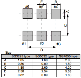
Product Name (Standard form)
External dimensions
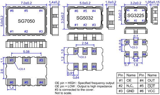
(Unit: mm)
Footprint (Recommended)
(Unit: mm)
To maintain stable operation, provide a 0.01 µF to 0.1 µF by-pass capacitor at a location as near as possible
to the power source terminal of the crystal product (between VCC - GND).
SHENZHEN YANGXING TECHNOLOGY CO., LTD.
ADD:Rm 1901, 19th Floor, 1st Huide Building, Mintang Rd No.385, Longhua District, Shenzhen China
Email:export@yangxing.hk
Skype ID: 125784862


