Email:export@yangxing.hk
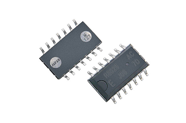
RX-8025SA
FIXED FREQUENCIES: 32.768KHz
PACKAGE: 1000 pieces/Reel
PROMISE: Lifetime warranty and technical support
ROHS STATUS: Compliant
PACKAGE: 1000 pieces/Reel
PROMISE: Lifetime warranty and technical support
ROHS STATUS: Compliant
 Download PDF
Block diagram
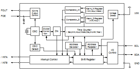
Overview
- Features built-in 32.768kHz crystal unit
- Frequency adjusted for high accuracy.
(±5×10⁻⁶ / Ta=+25°C)
(Equivalent to 13 seconds of monthly deviation)
- Frequency adjusted for high accuracy.
- The various detection function
- Power supply voltage monitoring function
(with selectable detection threshold) - Stop detection function
- Power-on reset detection function
- Power supply voltage monitoring function
- Alarm function and Periodic interrupt function
- The periodic interrupt outputs
- Dual Alarm function.
(Date of the week , Hour , minute)
(Month, Day, Hour, Minute )
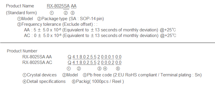
Specifications *Refer to application manual for details.
Recommend Operating Conditions
| Item | Symbol | Condition | Min. | Typ. | Max. | Unit |
|---|---|---|---|---|---|---|
| Power voltage | VDD | - | 1.7 | 3.0 | 5.5 | V |
| Clock voltage | VCLK | - | 1.15 | 3.0 | 5.5 | V |
| Operating temperature | TOPR | - | -40 | +25 | +85 | °C |
Frequency characteristics
| Item | Symbol | Condition | Rating | Unit |
|---|---|---|---|---|
| Frequency tolerance | Δ f/f | Ta=+25°C VDD=3.0V |
AA: 5±5 *1) AC: 0±5 *2) |
×10-6 |
| Oscillation start-up time | tSTA | Ta=+25°C VDD=2.0V |
1 Max. | s |
| Frequency voltage characteristics | f/V | Ta=+25°C VDD=2.0V to 5.5V |
±1 Max. | ×10-6 |
*1) 2) Equivalent to ±13 seconds of monthly deviation (excluding offset).
Current consumption characteristics
Ta=-40°C to +85°C
| Item | Symbol | Conditions | Min. | Typ. | Max. | Unit | |
|---|---|---|---|---|---|---|---|
| Current Consumption | lBK | fSCL=0Hz FOE=GND FOUT;output OFF(LOW) |
VDD=5V | - | 0.60 | 1.80 | µA |
| VDD=3V | - | 0.48 | 1.20 | ||||
| l32k | fSCL=0Hz VDD,FOE=5.5V FOUT;output ON (Output=OPEN;CL=0pF) |
VDD=5.5V | - | 3.0 | 6.5 | µA | |
Power supply detection voltage
Ta=-30°C to +70°C
| Item | Symbol | Condition | Min. | Typ. | Max. | Unit |
|---|---|---|---|---|---|---|
| High-voltage mode | VDETH | VDD pin | 1.90 | 2.10 | 2.30 | V |
| Low-voltage mode | VDETL | VDD pin | 1.15 | 1.30 | 1.45 | V |
Pin function
| Signal Name | Input/Output | Function | |||||||||||||||||||||
|---|---|---|---|---|---|---|---|---|---|---|---|---|---|---|---|---|---|---|---|---|---|---|---|
| SCL | Input | Serial clock input pin | |||||||||||||||||||||
| SDA | Bi-directional | Data input and output pin | |||||||||||||||||||||
| FOUT | Output |
32.768kHz clock output pin with the output control function. (C-MOS)
|
|||||||||||||||||||||
| FOE | Input | ||||||||||||||||||||||
| / INTA | Output | Interrupt output A pin (N-ch open drain) | |||||||||||||||||||||
| / INTB | Output | Interrupt output B pin (N-ch open drain) | |||||||||||||||||||||
| TEST | - | *Used by the manufacture for testing. (Do not connect externally.) |
|||||||||||||||||||||
| VDD | - | Connected to a positive power supply. | |||||||||||||||||||||
| GND | - | Connected to a ground. |
Terminal connection / External dimensions
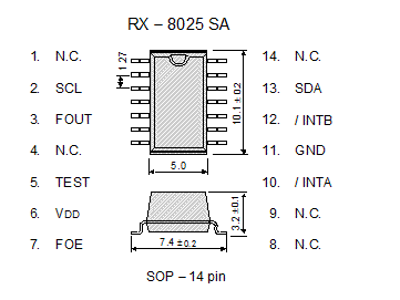
(Unit: mm)
The metal case inside of the molding compound may be exposed on the top or bottom of this product.
This purely cosmetic and does not have any effect on quality, reliability or electrical specs.
Footprint (Recommended)
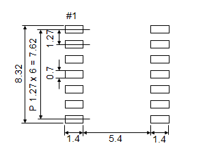
(Unit: mm)
To maintain stable operation, provide a 0.1uF by-pass capacitor
at a location as near as possible to the power source terminal of the crystal product (between Vcc - GND).
SHENZHEN YANGXING TECHNOLOGY CO., LTD.
ADD:Rm 1901, 19th Floor, 1st Huide Building, Mintang Rd No.385, Longhua District, Shenzhen China
Email:export@yangxing.hk
Skype ID: 125784862


